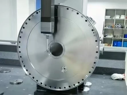
CNC Machining Services For The Semiconductor Industry

Semiconductor equipment depends on vacuum-tight interfaces, particle-conscious surfaces, stable hole patterns and flatness controlled across substantial parts. We machine critical components for wafer processing, handling, gas delivery and test equipment, with material discipline, planned inspection and documentation aligned with your drawing and purchase order.

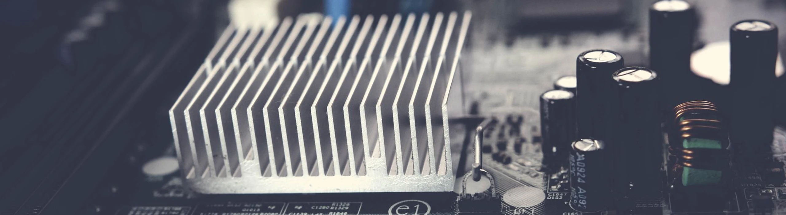
Aluminum finned heat sink mounted on an electronic circuit board beside capacitors

CNC Machining For The Semiconductor Industry

Behind every wafer fabrication tool is a supply chain of precision-machined hardware: chambers where deposition and etch processes occur, end effectors that move wafers, manifolds that deliver process gases and fixtures that keep assemblies aligned.

These components operate under high vacuum, plasma exposure, aggressive cleaning chemistry and cleanliness requirements where an uncontrolled burr, residue film or damaged sealing face can affect equipment performance. Geometry and surface condition therefore have to be planned as one manufacturing problem.

We support semiconductor equipment OEMs, subsystem builders and maintenance teams with prototype iterations, first-article builds, recurring production and drawing-controlled replacement parts. The machining route, finishing allowance, inspection method and required records are reviewed before release.

Customer-specific SEMI requirements, leak-test limits, particle criteria, cleaning instructions and packaging standards must be supplied with the RFQ so they can be included in the agreed manufacturing and verification scope.

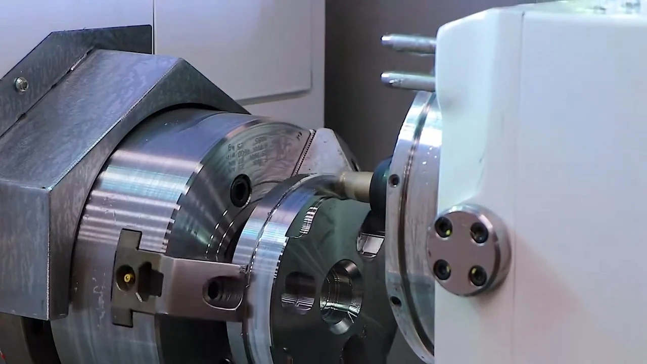
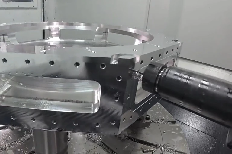
CNC spindle machining side features on a large metal housing with a circular opening

Types Of Semiconductor Parts We Manufacture

Parts are manufactured to the released drawing, with vacuum interfaces, cleanliness-sensitive geometry, hole patterns, material identity and post-process requirements reviewed as connected characteristics.

The Challenges Of Semiconductor Parts Machining

A dimensional report is only one part of release. Semiconductor hardware also depends on burr condition, surface integrity, material behavior, contamination control and protection through downstream processing and shipment.

Final capability is confirmed against the released drawing. Part size, stock condition, wall geometry, datum structure, material behavior, finishing allowance and measurement access can materially change the manufacturing route.

Particle And Burr Control

Blind holes, intersecting passages and small edges are reviewed before programming so deburring and cleaning access are part of the machining route rather than a final correction.

Sealing-Surface Finish
Specified Ra values are planned with the cutting or finishing route and verified with appropriate surface measurement.
Cleanliness Requirements
Customer particle, residue, cleaning and packaging specifications are incorporated when supplied with the RFQ.
Manufacturing Processes For Semiconductor Components

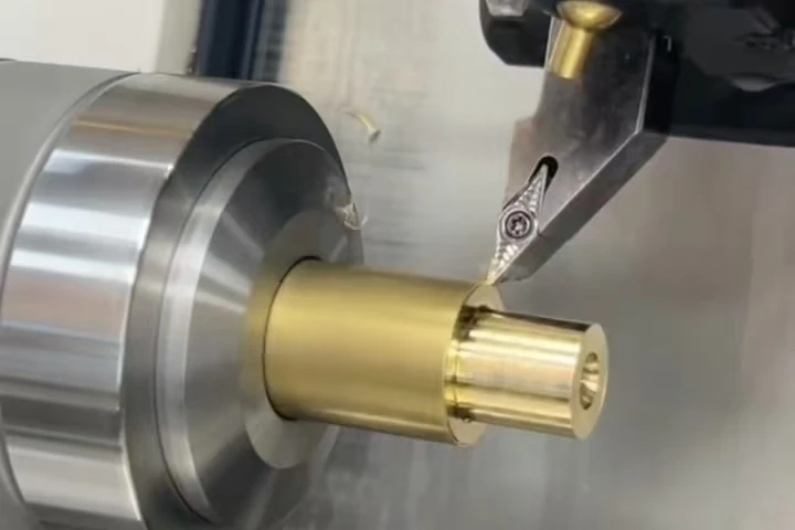
Our semiconductor component manufacturing processes include CNC milling, CNC turning, mill-turn machining and Swiss machining. Engineering review selects the route around geometry, material, sealing interfaces and inspection requirements.

CNC Milling

Use 3-axis and 5-axis milling for chambers, plates, manifolds and multi-face structures. Datum continuity, wall stability and tool access are planned for sealing grooves, precision hole patterns and intersecting passages.

  • Large Plates And Chambers
  • Multi-Face Feature Control
  • O-Ring Grooves
  • Precision Hole Patterns
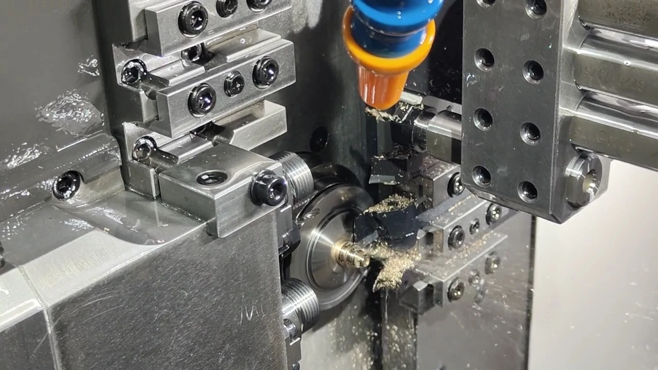
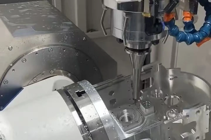
CNC milling spindle cutting a metal workpiece on a rotary fixture

How Our Semiconductor CNC Machining Service Process Works

The manufacturing sequence covers drawing and technical requirements review, process planning, incoming material inspection, first article inspection, production machining, surface treatment and final inspection. Machining instructions and inspection records are tied to the approved drawing revision and production batch.

Engineering Review

  1. 01

    Drawing Submission

    Provide the STEP model and dimensioned drawing with the current revision, material grade, quantity, surface finish, required delivery date and inspection requirements. Where required, an NDA is signed before drawings and models are exchanged.

  2. 02

    DFM Review

    Review geometry, dimensional and geometric tolerances, stock condition, tool access, workholding and measurement access. Identify features that affect machining feasibility, dimensional stability or inspection, and resolve proposed drawing changes with your engineering team.

  3. 03

    Technical Requirements Review

    Confirm the drawing revision, material specification, datum scheme, critical dimensions, surface finish and inspection requirements. Resolve drawing queries and document approved changes. Prepare the quotation from the confirmed part requirements, quantity and delivery schedule.

Production Preparation

  1. 04

    Semiconductor CNC Machining Process Planning

    Define the operation sequence, machining datums, fixtures, cutting tools and cutting parameters. Prepare the NC program and inspection plan, review toolpaths through machine simulation, and establish the setup instructions for the first-article machining trial.

  2. 05

    Material Procurement

    Specified material grades and stock forms are purchased exclusively from approved or qualified suppliers, matched to the requirements of your drawing and purchase order.

  3. 06

    Incoming Material Inspection

    Check stock identification, dimensions, surface condition and material certificates against the specified grade, condition and purchase order. Record the heat or batch number and link the accepted material to the production work order.

Controlled Machining

  1. 07

    First Article Inspection

    Machine the first article using the planned NC program, fixtures and tools. Inspect drawing characteristics with the specified measurement methods, record the results and correct setup or program deviations before batch production begins.

  2. 08

    Production Machining

    Run the approved Semiconductor CNC machining program with the documented fixture setup, tooling and cutting parameters. Maintain the specified datums and machining sequence, and record approved changes to programs, tool offsets or setup instructions.

  3. 09

    In-Process Inspection

    Measure critical dimensions and geometric characteristics at the intervals defined in the inspection plan. Monitor tool wear and dimensional trends, adjust offsets where appropriate, and recheck affected features after adjustment.

Verified Delivery

  1. 10

    Machined Part Inspection

    Check the completed machining operations against the drawing and review the in-process inspection results. Record dimensional conformity and segregate nonconforming parts before the batch proceeds to finishing or other subsequent operations.

  2. 11

    Post-Machining Operations

    Complete the specified deburring, grinding, polishing, surface treatment or heat treatment. Check treatment records and reinspect features affected by material removal, coating thickness or heat-treatment distortion.

  3. 12

    Final Inspection And Shipment

    Inspect finished parts against the drawing and final inspection plan, including dimensions, surface condition and finish requirements. Compile the required material certificates and inspection reports, verify quantity and identification, then pack parts to prevent damage during shipment.

Materials For Semiconductor Components

Material selection affects vacuum behavior, corrosion resistance, thermal response, electrical performance, plasma exposure and dimensional stability. Grade, stock form and certification requirements are confirmed before procurement, with no substitution without written approval.

Showing 4 Materials: Metals.

Aluminum

  • 6061-T6
  • 6063
  • stress-relieved plate

Low density, high thermal conductivity and strong machinability; stock condition and porosity risk are reviewed for vacuum-facing parts and large plates.

Typical Applications

Chamber bodies, lids, structural plates, manifolds and anodized equipment components

Stainless Steel

  • 304L
  • 316L

Low-carbon grades support welded vacuum hardware; 316L adds resistance to chloride-bearing process and cleaning environments.

Typical Applications

Gas delivery hardware, vacuum weldments, wetted components and electropolished surfaces

Copper

  • C101 OFHC
  • C102 OFHC

High electrical and thermal conductivity with purity appropriate for vacuum and thermal-management applications.

Typical Applications

Thermal components, RF contacts, electrodes and conductive interfaces

Titanium

  • Grade 5 (Ti-6Al-4V)

High strength at low weight with strong corrosion resistance for specialized equipment and motion hardware.

Typical Applications

High-strength handling components, fixtures and corrosion-resistant interfaces

Surface Finishes And Cleanliness Control

In semiconductor applications, coating, masking, surface texture, residue removal and packaging can be functional requirements. Each process is quoted against the supplied specification and critical features are rechecked when post-processing can affect them.

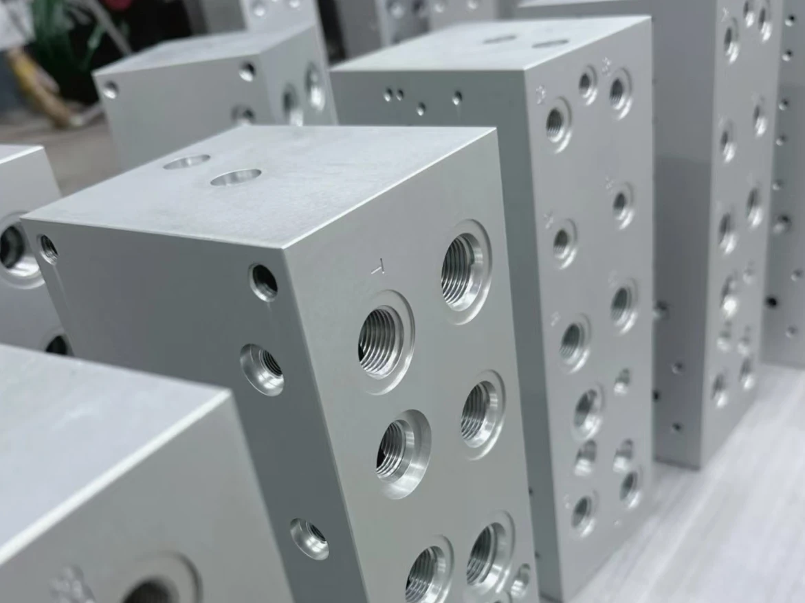
Natural-colored anodized metal blocks with threaded bores and side holes

Anodizing (Type II)

Natural or custom color; masking and thickness per drawing

A controlled oxide layer provides corrosion protection and electrical insulation on aluminum. Clear natural or custom dyed color is specified to the application; critical dimensions and sealing surfaces remain protected by the agreed masking plan.

Typical Applications

Chamber exteriors, structural plates and equipment frames

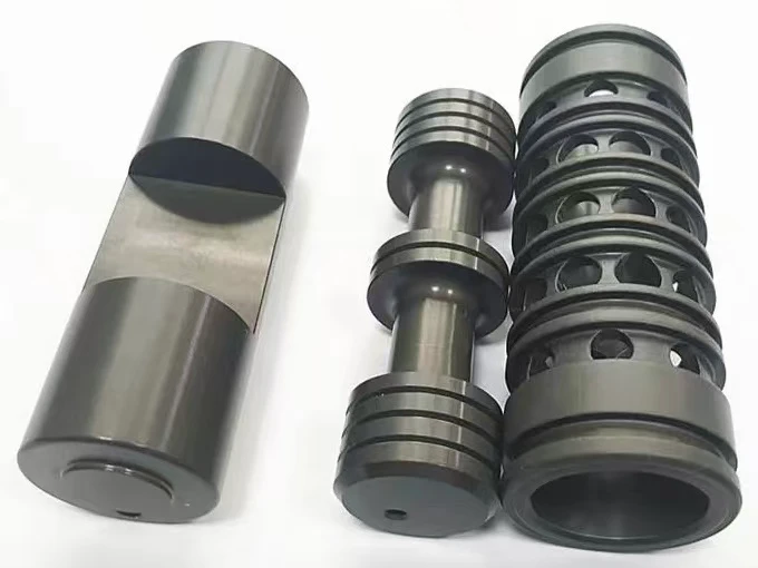
Dark hard-anodized cylindrical parts with grooves, shoulders and machined flats

Hard Anodizing (Type III)

Type III; thickness and sealing per drawing

A denser oxide layer improves wear resistance on aluminum parts. Coating allowance, edge condition and masking are specified during machining process planning.

Typical Applications

Wear surfaces, handling components and selected chamber hardware

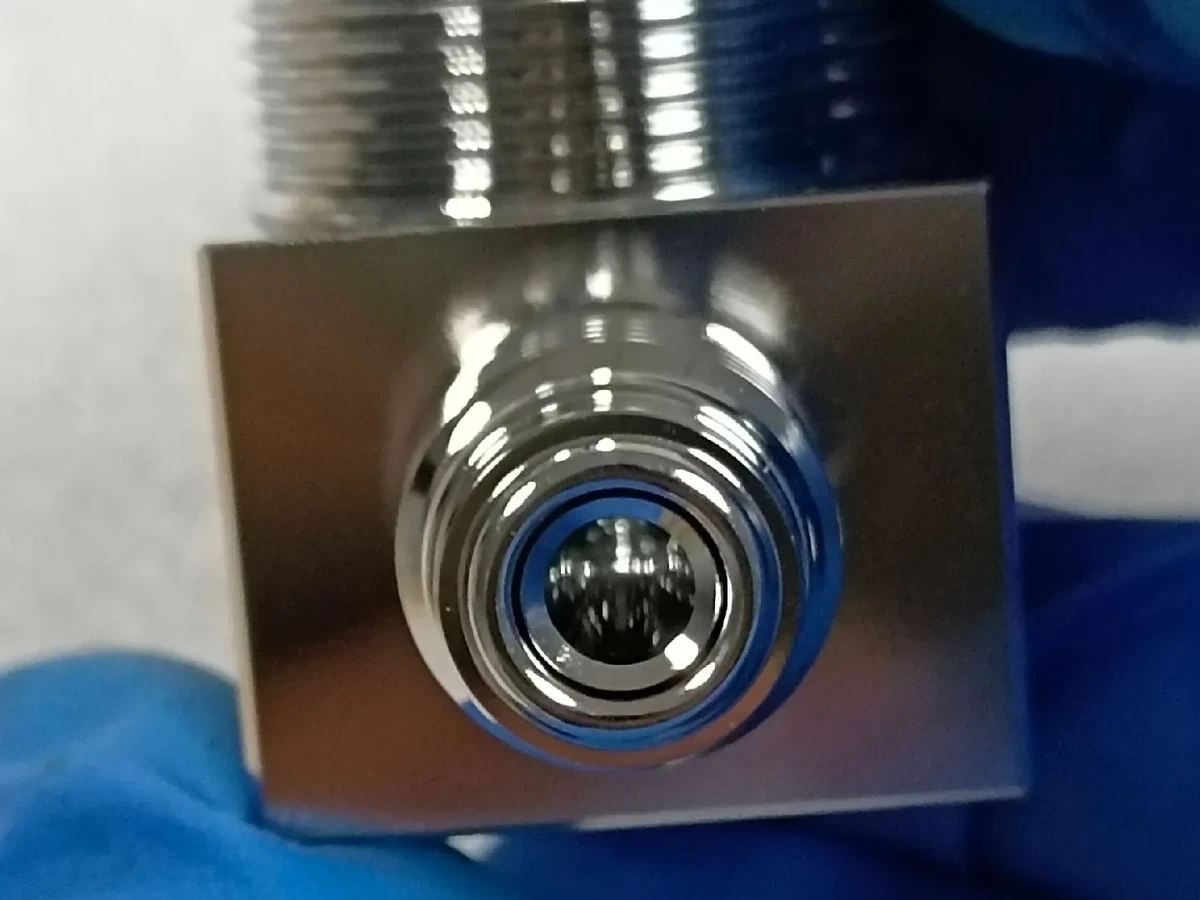
Electropolished metal fitting with a reflective square body, central bore and threaded boss

Electropolishing

Customer-specified surface and acceptance criteria

Electrochemical removal smooths stainless surfaces and can reduce microscopic burrs and embedded surface contamination when coordinated with a qualified source.

Typical Applications

Gas delivery and wetted stainless components

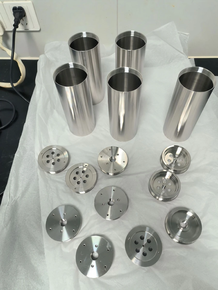
Stainless cylindrical housings and circular end plates arranged on a white sheet

Passivation

ASTM A967 when specified

Chemical treatment removes free iron from machined stainless surfaces and supports restoration of the protective chromium-rich oxide layer.

Typical Applications

304L and 316L vacuum or fluid-service hardware

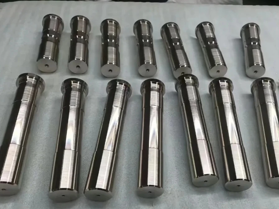
Nickel-finished metal shafts with stepped diameters arranged on a white sheet

Electroless Nickel Plating

Drawing-specified alloy, thickness and masking

Chemical deposition provides relatively uniform coverage on complex aluminum geometry while improving corrosion and wear resistance.

Typical Applications

Aluminum manifolds, chambers and internal geometry requiring controlled coverage

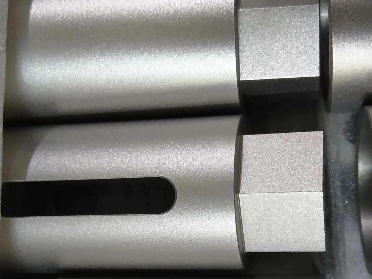
Matte-textured cylindrical metal components with flats and a longitudinal slot

Bead Blasting

Controlled media and finish standard

A controlled abrasive process produces a uniform matte texture where handling, optical or later coating requirements call for it.

Typical Applications

Equipment surfaces and coating preparation

Quality Assurance For Semiconductor Programs

Standard machining inspection verifies dimensions. Semiconductor quality assurance must also verify the surface condition, vacuum integrity, cleanliness and traceability that determine whether a component can perform in the fab environment.

If your quality team works to SEMI standards or maintains its own incoming-inspection protocols, send the specification with your RFQ. The inspection methods, acceptance criteria and documentation package are quoted directly to those requirements.

Why Choose Us For Your Semiconductor Program?

One engineering team connects drawing review, process selection, machining, qualified finishing, inspection, cleaning requirements and release documentation from development quantities through recurring production.

Engineering-Led Quotation

Review the machining sequence, fixtures, surface-treatment allowances, measurement access and required inspection reports before preparing the quotation.

Vacuum And Cleanliness Planning

Sealing geometry, internal passages, burr access, surface requirements, cleaning and protective handling are considered as one route.

Flatness And Hole-Pattern Control

Stock condition, balanced machining, in-process checks and CMM verification support large plates and dense positional requirements.

Semiconductor Material Discipline

Specified aluminum, low-carbon stainless, polymers, ceramics and OFHC copper are purchased to the drawing with lot traceability and no unapproved substitution.

Finishing Through Delivery

Machining, qualified finishing, post-process verification, cleaning and packaging can be coordinated under one purchase order.

Inspection And Conformance Records

Compile the specified dimensional inspection reports, material certificates, surface-treatment certificates, cleaning records and certificates of conformance for the delivered production batch.

Frequently Asked Questions

Practical answers about semiconductor component scope, vacuum requirements, materials, cleanliness, documentation and quoting.

What Semiconductor Equipment Parts Do You Machine?

Typical work includes chamber components, gas manifolds, wafer-handling hardware, distribution plates, showerheads, structural plates, test fixtures and drawing-controlled replacement parts.

Can You Support Large Chamber-Plate Flatness?

Yes, subject to drawing review. Material condition, part size, stock allowance, wall geometry, fixturing and the finishing route determine whether milling is sufficient or grinding and lapping must be included.

Do You Machine Semiconductor-Grade Plastics?

We review PEEK, PCTFE, PTFE, POM, Vespel and ESD-safe polymers against temperature, chemistry, outgassing, tolerance and handling requirements.

What Cleaning And Packaging Requirements Can You Support?

Cleaning, DI-water rinsing, drying and cleanroom-compatible packaging can be quoted to the customer specification. Include the cleanliness level, prohibited materials and receiving standard with the RFQ.

Can You Support Vacuum-Critical Components?

Vacuum-facing materials, sealing surfaces, O-ring grooves, weld preparations and internal passages are reviewed during DFM. Any required helium leak test method and acceptance limit must be defined with the RFQ.

Can You Handle Development And Production Quantities?

Yes. Prototype iterations, first-article builds and recurring production can follow one controlled route, with drawing revisions and process changes reviewed before release.

What Quality Documentation Is Available?

Material certificates with lot traceability, FAI reports, dimensional inspection records, surface-finish results, finish certificates, cleaning records and certificates of conformance can be supplied when agreed at quotation.

Can We Put An NDA In Place Before Sending Drawings?

Yes. An NDA can be completed before drawing exchange so geometry, equipment interfaces and process information are reviewed under the agreed confidentiality terms.